

• PCB Assembly.

    MKC | Development | Assembly: in-house | PCB assembly

PCBs are assembled on one or both sides using SMD, THT, or mixed components—reliably and to high mass-production standards.

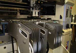
Fully automated assembly systems are used for SMD production. This ensures consistently high quality, efficient processes, and cost-effective production.

New technologies and package types are first introduced and tested on our own products. This ensures that proven processes and valuable experience are available before customer projects enter production. The result is functional, high-quality assemblies right from the start.

  • SMD, THT, and Mixed Assembly
  • Single-sided and double-sided PCB assembly
  • Fully automated SMD assembly
  • High production quality and process reliability
  • Proven technologies and enclosure designs
  • Customers benefit from tested processes
  • Customizable manufacturing requirements
MKC | Development | Assembly: in-house | PCB assembly

Assembly and Bill of Materials.

During PCB assembly, we can easily handle both single-sided and double-sided printed circuit boards with SMD components, conventional through-hole components (THT), and/or a combination of both.

To ensure high-quality mass production (SMD), we rely on fully automated placement machines.

We implement new production processes and technologies, as well as the use of new package types, in our own products. This ensures that our customers can be confident we have gained the necessary experience for error-free manufacturing and that they receive fully functional assemblies right from the start.

Below, we have compiled some information to help ensure a smooth manufacturing process. These are intended as suggestions and may vary depending on customer requirements.

As described for the printed circuit board, certain general conditions for the placement of components on the printed circuit board should be observed in order to enable high-quality and therefore error-free assembly.

In the case of double-sided assembly, it is important to ensure that the “heavy” components are placed on one side of the PCB in order to avoid additional costs, for example for the required adhesives or other rework.

The CAD data for placing the components to be assembled (pick and place) with the following information is desirable for data creation on our pick and place machines:

  • Unit of measurement used (mm, inch, etc.)
  • The origin point (ZERO) of the coordinates refers to the bottom right-hand corner of the PCB. If this deviates from your data, we need the offset to this point
  • Dimensions of the PCB
  • In the case of a multiple panel, we require a description of the structure and dimensions
  • X/Y coordinates of the reference marks
  • For each component to be assembled:
    • X/Y coordinate (centre point)
    • Assignment to the parts list (DIN designation: C1, IC2, R34, L5, D34, etc.) with component designation, value and housing.
    • Labelling if a component in the data is not to be assembled.
    • Designation of whether it is an SMD or THT component.
    • Rotation to the zero axis in degrees anti-clockwise
    • Designation on which side the component is assembled

In principle, this work can also be carried out manually, with the parts list and the assembly plans virtually on foot. However, this should be avoided for quality and cost reasons.

To enable fast and error-free preparation of your parts list, you should provide it to us as a table (Excel, OpenOffice) or as a CSV (Comma-Separated-Values) text file. The list should contain at least the following information for each component:

  • Sequence number of the component in the list
  • Quantity/number
  • Component designation and housing
  • Manufacturer and manufacturer designation
  • Assignment to the assembly plans (DIN designation: C1, IC2, R34, L5, D34, etc.)
  • Designation of whether it is an SMD or THT component
  • Farnell, RS or DigiKey number (optional or for prototypes)

Circuit Boards.

Regardless of the requirements that the development places on a printed circuit board, there are a few points to consider in order to be able to carry out high-quality and cost-effective assembly.
In this document, we explain the framework conditions for the printed circuit board and the multiple panel in order to ensure an optimised production process on our pick-and-place machines.

Procurement of circuit boards on behalf of the customer

So that we can order the circuit board for you, we need

  • the Gerber data for the printed circuit board or the multiple use,
  • the Gerber data for the paste film,
  • the drill list and
  • the information on the board structure (layer thickness and spacing, etc.) from you.

Provision of the circuit boards by the customer

If you would like to provide the PCB, we assume delivery in the original packaging supplied by the manufacturer at least 5 AT before the agreed delivery date.
To enable us to assemble the PCB, we require the data for creating the SMD solder paste stencil for each side of the PCB to be assembled. In order to avoid delays in delivery, it is desirable that you provide us with the Gerber data at least 8 AT before the agreed delivery date.

Dimensions

The dimensions of the printed circuit board or multiple PCB are limited to a maximum width of 290 mm and a maximum height of 250 mm.
The outer edges should be parallel to each other and straight to enable simple contour processing.

SMD.

In order to guarantee high-quality series production, the application of the solder paste or adhesive for the components is an important step in the SMD production process chain. For this reason, we use laser-cut stencils and semi-automatic printing systems with a vision system and stencil cleaning in this area.

We use several fully automatic placement machines for placement. We currently process more than 25,000 components per hour, from 0402 chips to fine-pitch QFPs and micro BGAs.

Depending on customer requirements, we can use both conventional convection reflow soldering systems and new vapour phase soldering systems for the soldering process. The temperature profiles used are of course monitored with internal oven sensors and regularly checked and logged with external temperature measuring devices.

Placement is possible from a component size of 0402 (metric 1005, EIA0402) and can be carried out on one or both sides.

The largest component we currently process is a BGA measuring 40 x 40 mm with micro-holes in the pad area. The pad spacing (pitch) should not be less than 0.8 mm.

For micro BGAs, reference marks, as described under printed circuit boards, are desirable to enable visual control of the assembly.

THT.

In most production orders for electronic assemblies, conventional or wired components (THT, through-hole technology) are used in addition to SMD components.

These components are soldered or press-fitted (PressFit) manually or using one of our wave soldering systems, depending on the customer’s wishes, complexity or requirements. The necessary presses and counterparts for press-fit components are available in many cases; we obtain any additional counterparts and/or tools that may be required from long-standing partners at short notice.

  • Wave soldering
  • leaded (pb-containing) and lead-free (pb-free)
  • Selective soldering
  • Soldering by hand
  • Press-fitting of components (PressFit)

When soldering, we use NoClean soldering tins to avoid additional cleaning of the assemblies.

Since the introduction of the RoHs guidelines, only RoHs-compliant materials and lead-free solders may be used. However, the legislator has authorised transitional periods for assemblies in defined areas of application. For this reason, we can also manufacture your assemblies with leaded materials if required.

Prototypes.

Our many years of experience in the areas of development and production, including the wide range of services we provide for our customers, show us how important the rapid assembly of prototypes and pre-production series is.

Based on this realisation, we have concluded framework agreements with our suppliers. We make these available to you in the form of a quick service.

Both single-sided and double-sided SMD boards, PCBs with conventionally wired components (THT) or mixed assembly are possible without any problems.

In order to guarantee series quality for the assembly of SMD components, we assume assembly with fully automatic assembly machines. If you require manual assembly, PCBs with other technical specifications or other deviations from these general conditions, please contact us.

Ideally, you will receive your assembled prototype, including PCB and material procurement, within 10 working days. If you provide the PCB and/or the components, delivery times of 48 hours after receipt of the material are also possible.

Series.

In general, we can support you in the area of “Electronic Manufacturing Services (EMS)” with the following services:

  • Production according to IPC-A-610 DE
  • Complete material procurement
  • Warehousing for e.g. “just in time” deliveries
  • Data transfer from common CAD systems
  • SMD-, THT– and mixed assembly of 1- or 2-sided PCBs
  • Programming of logic components (e.g. CPLD)
  • In-circuit programming and testing of components and assemblies (Boundary Scan, IEEE1149.1, JTAG)
  • Optical inspection
  • Electrical inspection with provision of the test setup
  • Development and production of a customized test setup

Redesigning circuit boards makes sense from a manufacturing point of view, even for small series, if this can save costs. Simply contact us, our development department will be happy to help you